LED displays have become ubiquitous by leveraging a simple yet powerful principle. Our eyes perceive full-color images when red, green, and blue (RGB) light mix in varying proportions. Add in the human eye’s “visual persistence” , and fast-paced scans of RGB LED pixels create the illusion of smooth, continuous motion.
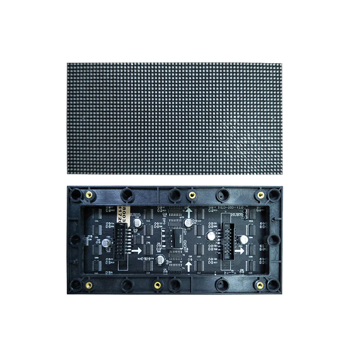
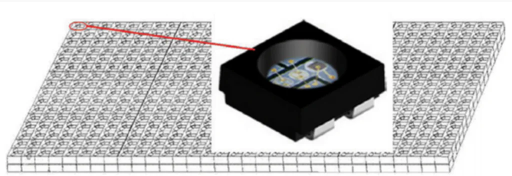
Every color pixel in a LED display relies on three independently controlled RGB LEDs working in tandem. But as the LED industry matures and demand for ultra-high-definition, high-density, and small-pitch screens grows, traditional packaging methods are hitting their limits. Today’s Below P2.5 small-pitch LED displays demand precision and reliability. The SMD 3-in-1 LED packaging can’t consistently deliver. So, how to solve these issue.
What is SMD packaging?
It refers to pre-assembled RGB LEDs are soldered onto a module substrate via reflow soldering. It struggles with low yields, poor reliability, and heat dissipation issues in dense configurations.
So, what is COB packaging? It is a new technology. Mounting LED bare chips directly onto module substrates and encapsulates them as a single unit. With fewer manufacturing steps, lower costs, higher integration, and superior display quality, COB LED display is poised to become the go-to packaging solution for the next generation of high-density LED displays. Let’s break down how it works, its core components, and why it matters.
The Structure of COB-Packaged LED Modules
To understand COB’s advantage, we first need to address the flaws of traditional SMD packaging for small-pitch displays. Shrinking SMD LED sizes further is technically challenging, and from an electronics reliability standpoint, discrete component assemblies are far less reliable than integrated ones.
Improveing packaging integration is the key to improving the reliability of small-pitch LED modules. COB technology does exactly that.
COB redefines the LED display’s basic building block. Instead of individual SMD LEDs, the minimum display unit becomes a COB module. Here’s how it’s structured:
We mount bare RGB LED chips directly onto a display module’s circuit substrate , establish electrical connections, secure them mechanically, and add heat dissipation and optical pathways. The end result is an integrated, display-ready component.

A high-integration COB LED module has three core parts:
- The PCB
- Driver chip circuits
- Array pins on the back of the PCB, and the LED array on the front.
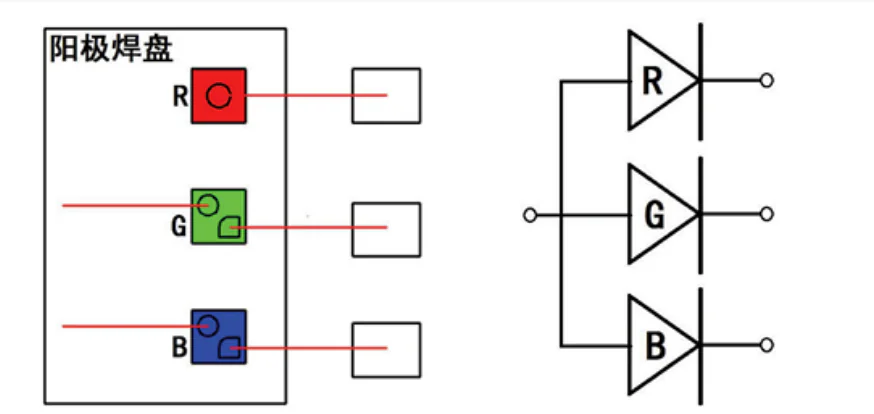
Each LED pixel unit contains three chips (R, G, B), four pins, and a common anode. We connect the RGB chips to their respective pins using gold wires, and the common anode also links to a pin via gold wire.
This pixel structure mirrors the internal RGB chip layout and circuit connections of traditional SMD 3-in-1 LEDs. For example, common anode configurations work seamlessly with existing LED display scan drivers, making COB compatible with current control systems.

The biggest structural win with COB? It combines traditional LED chip packaging and module substrate assembly into one step.
This simplifies the manufacturing process, reduces raw material use, and cuts costs. It also improves mechanical protection for LED chips:
- Improves reliability
- Enables pixel pitches under 2.0mm
- Supports mass production
- Enhances heat dissipation
- Minimizes “dead LEDs” .
The COB Module Packaging Process
To test if COB works for LED display manufacturing, our team designed and built a prototype COB module with a 2.0mm pixel pitch. Since COB mounts bare chips directly onto the substrate, the substrate itself must handle three critical jobs:
- Securing the chips
- Enabling electrical connections
- Ensuring consistent module alignment when tiled.
LED Bare Chips & Substrate Wiring

We selected specific RGB bare chips for the prototype:
- Vertical-structure reverse-electrode chips for red,
- Horizontal-structure Sapphire-substrate chips for blue and green.
To accommodate scan driving, we connected the anodes of the three RGB chips in each pixel via wire bonding. This common anode setup expands wiring space on the substrate。 It solves a major challenge in dense small-pitch designs.
Our substrate wiring design places the three chips on large pads, which provides ample space for die bonding while improving heat dissipation.
We soldered the chips’ cathodes to linearly arranged cathode pads, with five wires bonded per pixel.
Standardizing wire direction and length. Therefore, it significantly boosts yield rates by reducing human error.
Step-by-Step Packaging Flow
The COB packaging process follows a streamlined sequence:
- Wafer expansion
- Back gluing
- Die placement
- Curing, wire bonding
- Pre-testing
- Full-board molding
- Curing
- Final testing.
Let’s break this down in plain terms:
Wafer Expansion:
We use an expander machine to separate individual LED dies from the wafer.
Back Gluing:
We apply silver paste either to the expansion ring holding the wafer or directly to the substrate.
Die Placement (Dicing):
We Position each LED die onto the pre-glued substrate with precision.
Curing:
We Place the substrate in a thermal cycle oven to harden the silver paste
Wire Bonding:
We use gold wires to connect the LED chips to the substrate’s pins. It establishes the electrical connections needed for the chips to light up.
Pre-Testing:
We will check the module’s electrical performance early to catch and discard faulty units before final processing.
Full-Board Molding:
We place the entire substrate into a mold and inject thermally conductive encapsulant silicone.
Final Curing:
Harden the silicone in a controlled environment to ensure consistency.
Post-Testing:
Conduct a final electrical performance check to separate high-quality modules from defective ones.
Testing COB Modules: Key Quality Checks

Die bonding, wire bonding, and molding are the make-or-break steps for COB quality. Poor die bonding ruins subsequent wire bonding. For example, a poorly designed pad can leave gaps in the silver paste under the chip, leading to uneven wire tension and lower yields.
The ideal die bonding requires full silver paste coverage around the chip . Substrate design also impacts wire bonding difficulty and yield rates, so getting the PCB layout right is non-negotiable.
Full-board molding is particularly well-suited for LED display modules, as it ensures consistency, superior display quality, and high reliability.
The process is straightforward:
- Place the substrate in a mold,
- Pour liquid encapsulant,
- Cover with a lid,
- Cure at a constant temperature,
- Remove the finished module.
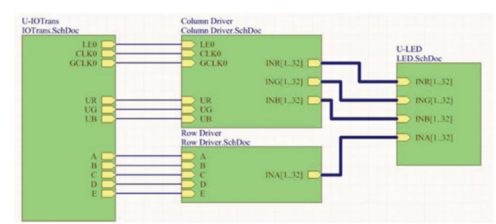
We tested our COB prototype using the same 1/32 dynamic scan driving method as standard SMD modules.
The results spoke for themselves: the COB module has excellent color consistency, high brightness, and precise array dimensional accuracy. It wll outperform many SMD equivalents.
To maximize yield and reliability, we also learned two critical lessons during testing:
- first, use LED chips from the same batch with matching optoelectronic properties.
- Second, optimize substrate design to support proper die bonding and wire bonding. It can cut corners here leads to costly rework and lower-quality modules.
Conclusion:
COB packaging solves many of the pain points plaguing traditional SMD 3-in-1 packaging for small-pitch LED displays. It has simple process, lower costs, superior display quality, high reliability, and long lifespan advantage .
Therefore, it is the ideal choice for high-end small-pitch applications. But to fully unlock COB’s potential, LED display manufacturers must focus on four key areas: rigorous testing and sorting of LED wafers to ensure uniform brightness and color; thoughtful substrate pad design to guarantee high-quality die bonding; optimized wire bonding parameters to boost yield; and consistent full-board molding to protect components and maintain display performance.
As the LED industry continues its march toward ultra-high density and ultra-high definition, COB packaging isn’t just a “nice-to-have”. it’s a necessity. It addresses the fundamental limitations of SMD technology while aligning with the industry’s goals of better performance, lower costs, and greater reliability.
For anyone investing in small-pitch LED displays, You should understand COB technology. it’s essential to staying ahead in a rapidly evolving market.
The bottom line? COB packaging is more than a technical upgrade. it’s a revolution in how we build LED displays. As the technology matures further, we’ll likely see COB become the dominant packaging standard for small-pitch and ultra-small-pitch LED displays in the years to come.