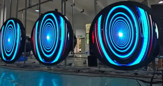
As people’s requirements for the display effect are more and more high-definition, “5G + 8K ultra-high definition” continues to develop, in the LED display industry, small-pitch LED display has also begun to break through the upper limit of the ultra-high-definition display, small pitch LED display and even micro-pitch LED display has become an inevitable trend of the industry development.
As we all know, the smaller the pitch of the LED display, the higher its resolution, which is also micron-scale Micro LED, Mini LED is known as the future of display technology. Micro LED, Mini LED product’s ideal technology is COB integrated packaging + full flip LED chip technology combination. Do you know the difference between SMD, IMD and COB LED packaging?
SMD LED Packaging technology:
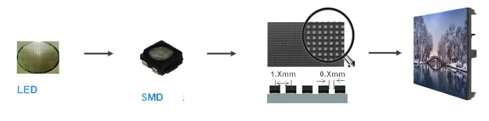
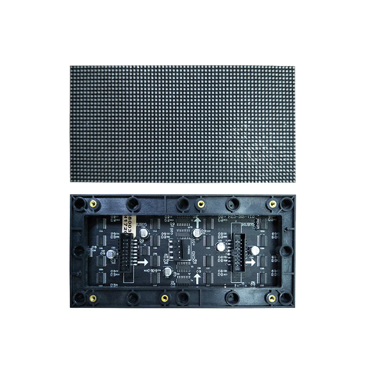
SMD is a surface-mounted device, the SMD LED packaging will be fixed in the bare chip on the bracket, through the gold wire will be electrically connected to the two, and finally protected by epoxy resin. SMD encapsulated lamp beads to the display manufacturers, through the reflow soldering soldering joints and PCB connection, and the formation of modules for assembly. SMD encapsulated small pitch products, generally exposed LED beads, or the use of masks
SMD Features:
- Using surface mount technology (SMT)
- the degree of automation is relatively high,
- It has a small size, large scattering angle,
- good luminous uniformity, and reliability.
COB LED Packaging technology:
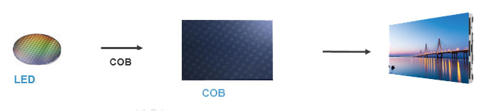
COB, chip-on-board packaging technology (Chip on Board). With SMD will beads and PCB welding are different.
COB process step:
- in the substrate surface with thermally conductive epoxy resin (silver-doped particles of epoxy resin) to cover the silicon wafer placement point,
- through the adhesive or solder will be LED chips with conductive or non-conductive adhesive adhesive in the interconnecting substrate.
- through the lead (gold wire) bonding to achieve the chip and the PCB board electrical interconnections between the LED wafers are fixed to the display substrate’s front surface, the film is pasted on the front surface of the display substrate.
The LED wafer is an ordinary red, green and blue LED light-emitting chip to realize the integrated package.
COB LED packaging Features:
- Compared with the SMD package, COB package small pitch has the smaller the density;
- Good thin, light, anti-collision pressure;
- Good flexibility;
- Good display Effect;
IMD LED Packaging technology:

IMD process still follows the surface mount process, combining the advantages of SMD, and COB.
From the pixel structure, the traditional SMD package is basically a pixel; COB package is the LED chip directly packaged into the module substrate, and then each large unit of the overall mold sealing, a package structure has hundreds of pixels;
IMD is “four in one”. there are four basic pixels in a package structure, the essence is still four by 12 RGB-LED chips synthesized “lamp beads”. In essence, it is still four “light beads” synthesized by 12 RGB-LED chips.
“Four-in-one” LED module is the chip is installed, with the packaging manufacturers to make more requirements for the chip, the latter may also launch “six-in-one” or even “N-in-one” LEDs.
IMD LED Packaging Features:
- It can be wavelength, brightness selection, and different molds out of the device in the tape before the uniform dispersion
- Effectively avoiding the encapsulation of subtle differences lead to paste the board after the emergence of local color difference,
- Better color consistency;
IMD vs. COB LED Display Comparison
In the field of P0.9 LED display, mainly focuses on the use of IMD and COB. So in terms of display effect and comprehensive cost between COB and IMD LED display, which will be more advantageous?
Display effect:
Ink color consistency
COB LED module color difference is more obvious, and the early IMD will also appear large angle pockmarks, but currently have been well resolved. And COB to solve the problem of color consistency, the cost is much higher than the N-in-one package IMD device
- cost IMD < COB;
- efficiency: IMD> COB
Color consistency
Due to the COB splicing seam optical differences, and the smaller the module, the more obvious, the COB LED package belongs to the mixed chip:
- Can not do the test sorting,
- Color consistency can not be guaranteed,
- Point by point correction can only be satisfied with the front,
- The left and right viewing angle of the color difference is larger.
IMD can be imported into the full test sorting, maximize the elimination of bad, and the brightness ratio can be 1:1.5 ~ 1:1.3.
Yield (PCB yield + process yield + rework efficiency / yield)
PCB yield:
COB:
- the smaller the dot pitch, especially below P0.7, the smaller the pad pitch of the carrier board,
- the higher the difficulty of the multilayer board process
- the lower the yield;
IMD:
- P0.5-P0.9, 2-layer boards can be met
- the PCB board process difficulty is greatly reduced.
Encapsulation process yield:
COB:
- the denser the lamp beads, the lower the passing rate
- To ensure that there are no bad spots before encapsulation must be repaired through the laser repair equipment to improve the total yield, the repair efficiency is low;
IMD:
- The process is mature,
- Defective products are rejected directly in the test session.
| Type | PCB Structure | Pad gap/μm | PCB Yield Rate | Single Batch Yield Rate | Repair efficiency |
|---|---|---|---|---|---|
| P0.9 | COB: 8 layers (FR4) | 100-150 | 70-90% | 70-80% | Low |
| IMD: 2 layers (BT) + 6 layers (FR4) | 100 | >95% | >98% | Test phase elimination | |
| P0.9 flip-chip | COB: 8 layers (BT/High Tg FR4) | 80-90 | 60-80% | 80-90% | Laser repair |
| IMD: 2 layers (BT) + 6 layers (FR4) | 80-90 | >95% | >98% | Test phase elimination | |
| P0.7/0.6 (Flip-chip | COB: 8 layers (BT/High Tg FR4) | 60-70 | 50-60% | 70-90% | Laser repair |
| IMD: 2 layers (BT) + 6 layers (FR4) | 60-70 | >90% | >95% | Test phase elimination | |
| P0.5/0.4 (Flip-chip) | COB: >10 layers (BT/High Tg FR4) | 30-50μm | 30-40% | 60-80% | Laser repair |
| IMD: 2 layers (BT) + 8 layers (FR4) | 30-50μm | 70-80% | >80% | Test phase elimination |
Reliability
Anti-bumping ability, IMD (P0.9) welding thrust value up to 2-3kg, can meet the leasing market demand
Maintenance difficulty :
- IMD (P0.9) and COB-P0.9 failure rate <10ppm, but IMD can be repaired on-site, directly replace the corresponding bad points with good products, lower maintenance costs;
- COB is difficult to repair and need to be repaired by replacing the module in a high-cost way.
Comprehensive cost aspects:
Color consistency cost
COB (resolution 16*16=256), theoretical concentration = 0.98^256=0.56%. Far lower than IMD 92.13%.
As COB integrated package the more chips, the higher the requirements of the chip segment. And it is necessary to use a narrower distribution of chip feeding to ensure better consistency.
Corrective technology can only guarantee the consistency of the front, there are still color differences at large angles. Therefore, COB in color consistency to pay the cost is higher than IMD.
Manufacturing costs
Take P0.9 as an example, the manufacturing cost is about 25-30% for COB and 10-15% for IMD.
If you want to reduce COB cost, the core is to improve the yield;
IMD is relatively more reducing the cost of space.
Comprehensive display effect and comprehensive cost comparison, For the P0.9 LED display, IMD has technology, cost, rapid industrialization of comprehensive advantages;
For P0.4-P0.7 LED display, IMD still occupies the first mover advantage due to flip COB facing yield, rework efficiency, cost, and other difficult to improve.
COB vs. SMD LED Display Comparison
Image differences
SMD LED screen: lamp beads are single-body light-emitting, showing the effect of point light source.
COB LED screen: due to the light-emitting chip above the overall film, the light source after the film scattering and refraction into the surface light source.
Compared with point light source, surface light source has a better overall visual perception, no particles when watching, and can reduce the stimulation of the light source to the human eye, which is more suitable for long-time close-up viewing.
COB LED screen using a new process after the overall package, the contrast ratio can be higher, up to 20,000:1 or more;
SMD LED screen contrast ratio will not be more than 10,000:1, compared to the front view when the COB screen viewing effect is closer to the LCD screen. It has good bright and vivid colors and better detail performance.
However, because the COB screen can not be like the SMD screen on the single lamp bead similar optical properties of the sorting, LED display factory needs to do the whole screen screen correction, although the front viewing effect is excellent, but a large angle when looking at the side of the phenomenon is prone to color inconsistencies.
Reliability differences
SMD LED screen:
- due to the light-emitting chip is first encapsulated and then mounted, the overall protection is weaker,
- Easy to knock the lights off the lights;
- waterproof, moisture-proof, dust-proof performance is poor,
- It can not be wiped, but the site is easy to repair, conducive to the maintenance of the later stage.
COB LED screen:
- The chip is directly mounted after the overall coating, the overall protection is better;
- the front protection level up to IP65,
- can be effective waterproof, moisture-proof, anti-knock,
- you can use a wet towel to clean, but due to the overall coating;
- the scene can not be repaired, you need to return to the factory to use professional equipment for maintenance, which is more inconvenient.
Difference energy efficiency
SMD LED screen
Within the lamp bead light-emitting wafer is mostly installed for the process, the light source above the lead blocking, while the COB screen is mostly installed for the process, the light source is not blocked, so to achieve the same brightness.
COB LED screen
Power consumption is lower, with a better use of the economic model.
In addition, because the epoxy resin used for SMD lamp bead package has a low transmittance, the overall film used for COB screen has a high transmittance, which further improves the economy of COB screen.
Cost Differences
SMD:
- SMD’s production technology and process is relatively simple;
- due to the low technical threshold, the country has more than a thousand manufacturers;
- competition is more adequate
- the development of technology is more mature.
COB:
- COB’s production process has a high technical threshold;
- there are only less than twenty manufacturers with R&D and manufacturing capabilities.
- COB technology is still in rapid development, although its theoretical cost is lower than the SMD screen。
- Due to lower product yields, the current cost of the COB screen compared to the SMD screen in more than 1.2 pitch still has a certain disadvantage.
Top LED display Manufacturers talk Below P1.0 LED display market: COB Vs. IMD Vs. SMD LEDs
Unilumin Technology
SMD packages LED screens typically have a dot pitch starting at P1.2. They face a development limit because they can’t achieve dot pitches below 1.0 mm.
COB packaging allows for smaller dot pitches. Unilumin Technology’s Mini and Micro series use mature COB technology, which minimizes lamp loss and greatly improves resolution and clarity.
Currently, COB-packaged mini LED display are gaining momentum. They are widely used in indoor projects due to their small pitch. Large-size standardized displays such as LED integrations and LED TVs are experiencing strong growth.
Another new display technology, Micro LED, is approaching mass production. As the global economy recovers, COB technology products could see significant market opportunities.
The high production threshold for COB packaging hasn’t yet allowed its widespread use.
However, the future market looks promising. High-resolution micro-pitch LED screens are ideal for close-up viewing. With cost reductions, these LED screens are expected to open up markets for integrated machines and consumer applications.
In the future, COB screens are likely to become central to the LED display industry, leading the way for small-pitch LED technologies.
Xida Electronics:
The era of high-definition has arrived, but the full potential of LED direct display is just beginning. Under national policies for green development and carbon reduction, and with tighter post-pandemic budgets, there’s a growing need for cost-effective, green, ultra-high-definition displays. This need is expected to shape future trends.
The best technical route for LED display less than P1.0 pitch is inverted COB. This technology not only offers superior picture quality, but also addresses safety, energy efficiency, environmental friendliness, high definition, health and reliability.
Inverted COB has become a new focus for investment, accelerating its technological development and market expansion.
SightLED:
COB technology is lowering the cost of sub-P1.0 applications and will eventually cost less than SMD. As COB displays become standardized for the 4K market, such as in-home theaters, we are seeing more and more P0.6 and P0.7 displays. This shift indicates a growing home theater market beyond the traditional commercial display market.
LianTronics:
As an important technology for micro-LED products, inverted COB packaging stands out in terms of display quality, reliability and environmental friendliness.
Demand for the below P1.0 LED display is shifting to mainstream products. COB LED displays offer advantages in display quality, performance, cost and supply chain, making them the future mainstream choice.
Absen:
Below P1.0 LED display market currently focuses on SMD, IMD, COB, and MIP technologies, with IMD and COB holding the largest market share. COB technology offers more stable protection and uniform, soft light display.
As COB technology matures and yield rates improve, it is expected to become the leading technology choice for below P1.0 applications.
Hikvision:
The market outlook for below P1.0, COB display products is positive. COB displays have achieved a higher penetration rate in the below P1.0 market, with applications such as command centers and high-end conference rooms showing significant growth.
As COB technology continues to mature and costs decrease, the advantages of COB LED displays in terms of softness, moisture resistance and shock resistance. Therefore it will continue to expand its market presence and challenge SMD LED display.
Conclusion:
Compared with IMD and SMD technology, as COB packaging technology is more mature, COB technology from the performance, safety, cost and other aspects of the advantages, most of the LED display manufacturers have deep plowing COB and advance the layout of the consensus.
COB LED display is now generally recognized in the command and control center, commercial display and other traditional areas of application, but also in the future in the naked eye 3D, AR/XR, home theater and other innovative areas also have broad prospects.