Het tijdperk van de mini-/micro-LED-schermen is aangebroken, maar om de populariteit van micro-pitch-schermen te realiseren, zijn opbrengst- en kostenbeheersing de sleutel tot massaproductie op grote schaal. De beste manier om te voldoen aan de opbrengst en kosten optimalisatie op hetzelfde moment is om te beginnen met het verpakkingsproces.
In het geval van COB LED-technologie heeft bezet de first-mover voordeel, MiP in 2023 versneld in de markt, een aantal top LED-display fabrikanten met behulp van MiP technologie.
Maar weet je het verschil tussen MIP en LED-technologie, wat is de marktpositionering en de toepassingsmogelijkheden van MiP en COB technologieën? Welke route heeft de voorkeur van de beste LED fabrikanten?
MiP (Micro LED-in-Package) Technologie:
MiP technologie verwijst naar de inkapselingsmethode waarbij micro-LED’s individueel of in kleine groepen worden verpakt voordat ze tot een display worden geassembleerd. Het kan de hoge precisie en flexibiliteit verbeteren bij het maken van displays met hoge resolutie.
Kenmerken:
- Hoge precisie
- Betere beeldschermconsistentie
- Verbeterde opbrengst
- Verbeterde betrouwbaarheid
- Kleinere chipgrootte
- Kostenefficiëntie
- Hoge helderheid en contrast
Toepassingen:
MiP technologie wordt gebruikt in verschillende toepassingen, waaronder smartphones, televisies, grote beeldschermen binnenshuis en andere beeldschermen met een hoge resolutie.
COB (Chip-on-Board) LED-technologie:
Bij COB-technologie worden meerdere LED chips rechtstreeks op een substraat gemonteerd om een enkele module te vormen. Deze LED chips worden vervolgens bedekt met een laag fosfor of inkapseling om een enkele lichtbron te creëren.
Kenmerken:
- Hoge lichtdichtheid
- Verbeterd thermisch beheer
- Compact ontwerp
- Minder verblinding
- Vereenvoudigde installatie
- Hoge efficiëntie
- Kosteneffectiviteit
- Gelijkmatige verlichting
Toepassingen:
COB LED’s worden gebruikt in een verscheidenheid aan toepassingen, waaronder downlights, straatverlichting, high bay armaturen, schijnwerpers en spots. Ze zijn ook populair in hoogwaardige residentiële en commerciële LED-displayoplossingen vanwege hun uniforme lichtopbrengst en efficiëntie.
Verschillen en voordelen van MiP en COB LED technologieën
COB en MIP hebben hun eigen verschillen en voor- en nadelen op het gebied van maakbaarheid, gebruiksscenario’s en displayprestaties:
LED-verpakking:MIP-technologie is een verpakkingstechnologie op chipniveau. Het neemt het idee van het veranderen van het geheel in nul, het verpakken van een heel paneel afzonderlijk, en het oplossen van het probleem van hoge opbrengst controle moeilijkheid in groot gebied door het beheersen van de opbrengst van klein gebied.
Maakbaarheid:MIP (Mini LED in verpakking) kan hergebruik SMD productie-apparatuur, minder zware activa investeringen; MIP (Micro LED in verpakking) kan in staat zijn om gedeeltelijk hergebruik SMD bestaande productie-apparatuur;
COB LED verpakking en display technologie, vermindering van een deel van het productieproces, hoge productie-efficiëntie, en MiP is hetzelfde als de traditionele SMD, de eerste uit het pakket, en doe dan de patch, twee productie schakels.
Maar MiP kan compatibel zijn met de huidige SMD surface mount apparatuur, overdracht kosten laag is, in staat om enkele chip aangepast aan verschillende substraten, verschillende pixel pitch toepassingen. COB (Chip on Board) is vereist om te investeren in een aparte productielijn, die een grotere kapitaalinvestering vereist.
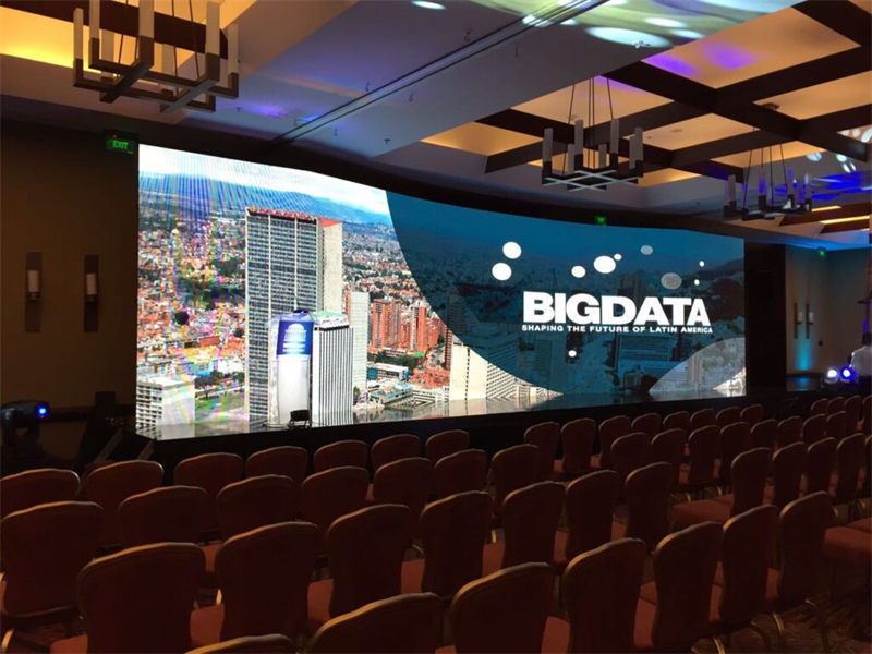
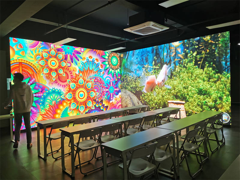
Toepassing: COB en MIP (Mini LED in package) wordt voornamelijk gebruikt voor grote displays, zoals controlekamers, grote vergaderzalen, tentoonstellingen en andere indoorscènes; MIP (Micro LED in package) chipgrootte wordt steeds kleiner, Micro LED zal voornamelijk worden gebruikt in kleine displays, zoals draagbare apparaten, Micro LED TV, auto display en andere scènes.
MIP: chip-level verpakking, single-chip verpakking kan bereiken gemengd kristal, spectrale, kleurscheiding, de huidige minimum kan doen P 0,9 pixel pitch.
COB: chip-on-board verpakking, hogere helderheid, betere warmteafvoer, goede betrouwbaarheid, kan P 0,4 en de volgende Micro-level pitch.
Weergaveprestaties: COB heeft gerealiseerd hoge helderheid, goede zwarte consistentie, hoog contrast kenmerken, kan goed aanwezig HDR-effect, display stabiliteit en ga zo maar door dan de traditionele SMD-producten hebben uitstekende voordelen, MIP (Mini LED in Package) display prestaties en COB is vergelijkbaar met de consistentie van de grote kijkhoek is beter dan de COB, zoals niet doen het oppervlak van het geïntegreerde pakket verwerking, display stabiliteit is niet zo goed als de COB.
MIP (Micro LED in pakket) is de huidige Micro LED relatief goede massaproductie van technologie routes, kan ultra-hoge resolutie display te realiseren, kan realiseren P0,4 mm onder het display producten, de aandrijving regeling van de nauwkeurigheidseisen zijn hoger, dus in de ultra-kleine pitch display zal beter zijn.
Productieproces: MIP moet nog steeds individuele lamp kraal apparaten inkapselen en vervolgens overbrengen naar de lamp boord door SMT of solid crystal. COB-technologie is een eenvoudiger proces waarbij meerdere LED-chips rechtstreeks op een printplaat worden geplaatst en vervolgens worden bedekt met een fosforlaag.
MIP versnelt de volwassenheid en toetreding tot de markt op een nieuw moment, van de traditionele LED direct display producten, de verpakking structuur omvat voornamelijk SMD, IMD en COB drie technologieën. Onder hen, als de meest volwassen technologie, SMD neemt nog steeds een belangrijke positie in het tijdperk van micro-pitch .
Kosten: COB-technologie in P1.2 LED-display en SMD is gelijkmatig afgestemd op P0.9, COB uitgebreide toepassing kosten dan SMD heeft een duidelijk voordeel van de COB om de kosten van beugel te elimineren op hetzelfde moment, kan de chip meer klein, 02 * 06mil (50 * 150μm), 02 * 05mil (50 * 125μm) en meer geminiaturiseerd!
Chip geleidelijk gelanceerd in massaproductie, kan worden in de bestaande premisse van hetzelfde lichteffect chip kosten blijven dalen, de huidige mainstream fabrikanten van rechte door middel van tarief van 40% -60%, om de productie-efficiëntie te verbeteren op hetzelfde moment, zullen de kosten naar verwachting verder worden geoptimaliseerd; als een laatkomer om de MiP, fundamenteel een mix van COB-technologie en SMD-technologie en innovatie, maar de kosten van sterke afhankelijkheid van de omvang van de steun, de huidige is nog steeds in de hoge positie en de productie rendementen Laag.
Efficiëntie: COB vermindert LED bump, statische elektriciteit, vocht en andere slechte. Pixel pitch kan tot 0,5 mm of minder, goede weergave-effect, hoge helderheid, hoog contrast, grote kijkhoek, verzwakt moiré. Hoge mechanische eigenschappen en weerbestendigheid. De rijmodus is flexibeler dan bij discrete apparaten en er kan een virtuele pixelopstelling worden gerealiseerd.
Flexibiliteit: MIP kan de kleurscheiding voltooien na het inkapselen van een afzonderlijk apparaat en de kleurconsistentie van het productdisplay zal sterk verbeteren in vergelijking met COB-producten. Vooral wanneer bekeken vanuit een grote hoek, lost het het probleem van kleurafwijking van COB-producten op. Bovendien kunnen MIP-producten in vergelijking met COB-producten worden gelokaliseerd, wat ook erg belangrijk is.
Display effect:MiP LED-pakket, kan het apparaat worden gesorteerd en gemengd Bin, display consistentie; COB-module met een grote kijkhoek, anti-collision en compressie, goede warmteafvoer, lage snelheid van slechte plekken, maar kan niet worden single-pixel spectrofotometrische screening, kan alleen worden gecontroleerd vanaf de bron van de chip.bCOB inkt consistentie, intelligente correctie en detectie van reparatie en andere aspecten van de uitdaging bestaat nog steeds.
Vooruitzichten: MIP- en COB-technologie zullen zich in de toekomst blijven ontwikkelen, maar hebben elk hun eigen focus; MIP-technologie kan nieuwe doorbraken betekenen op het gebied van kostenreductie. MIP-technologie kan nieuwe doorbraken betekenen op het gebied van kostenreductie, terwijl COB-technologie nog veel ruimte voor verbetering biedt op het gebied van warmteafvoer en stralingssterkte. Beide partijen zullen zich blijven verdiepen in de toepassingsgebieden waarin ze gespecialiseerd zijn.
LED-productlijn: MIP verhoogt de GAP pitch van de behuizing door een inkapselingsproces toe te voegen om de toepassing van kleinere LED-chips en een hogere opbrengst in het back-end te realiseren.
MIP is een nieuwe producttechnologie, het productieproces vereist een enorme hoeveelheid overdrachtsprogramma. Momenteel is de technologie is nog steeds in het stadium van continue verbetering, MIP maakt de industriële keten arbeidsdeling, neigt naar de traditionele SMD-producten. Het waferproces wordt voltooid door de waferfabriek en het MIP-inkapselingsproces wordt voltooid door de inkapselingsfabriek. Massief kristal en SMT worden voltooid door de LED-schermfabriek.
MIP lost de LED wafer miniaturisatie (onder 2 * 4) test sorteren, PCBBT draagkaart lijnbreedte afstand beperkingen veroorzaakt door de pixel miniaturisatie (onder P0.5). Lagere LED wafer kosten door gebruik te maken van kleinere LED wafer grootte.
MIP-apparaten boven 0404 zijn compatibel met de originele SMT montage-apparatuur van het scherm fabriek, de meeste van de fabrikanten van 0404 en de volgende maten nog steeds gebruik maken van blauwe film verzending, die vast kristal machine vereist om de stukken te raken. MIP overdracht efficiëntie is hoog, de overdracht van een enkele pixel op een moment, dat gelijk is aan 3 keer van de efficiëntie van de COB overdracht wafer. Gemakkelijk te splitsen BIN, mengen lichten, goede weergave uniformiteit. Groot zwart gebied en hoog contrast.
Echter, de opbrengst eisen voor het voorste deel van het pakket hoog is, in vergelijking met de SMD toegenomen proces (scherm fabrikanten moeten de apparatuur investeringen en secundaire potting over te dragen) is ook toegenomen de bijbehorende kosten.MIP als je aan de uitgebreide kosten (materialen en arbeidskosten) lagere voorwaarden, kunt u concurreren met COB. Bovendien, de RGB gestapelde MIP, maar ook voor de ontwikkeling van small-pitch apparaten om een nieuwe richting en ideeën.
COB na bijna een paar jaar van exploratie en inspanningen, in het proces en de kosten zijn de meest beknopte en efficiënte programma, de huidige technologie is ook meer volwassen, in de opgaande fase. COB product-industrie keten arbeidsdeling, wafer fabriek wafers, LED scherm fabriek en LED verpakkingsbedrijf fusie te bieden, op hetzelfde moment, de verpakking te voltooien, patch verwerkingsproces, het elimineren van de noodzaak voor LED-lamp testen sub-BIN, verpakking en transport, inspectie en andere schakels, om de algehele efficiëntie te verbeteren.
| Kenmerk | MiP Technologie | COB Technologie |
|---|---|---|
| Miniaturisatie | Kleinere verpakkingsformaten, behoudt helderheid en kleurconsistentie | Standaard miniaturisatiepad, hogere efficiëntie |
| Compatibiliteit | Naadloos uitbreiden van bestaande elektronische structuren | Vereenvoudigde processen, hogere efficiëntie |
| Lichtmenging | Uitstekende lichtmenging, hoge uniformiteit, geen Mura-effect | Goede lichtmenging |
| Testen en Reparaties | Vermindert testmoeilijkheden, elimineert kostbare reparaties | Vereist vooruitgang voor verbeterde opbrengst |
| LED Chip Grootte | Handelt chips kleiner dan 60μm, kleinste dot pitch | Standaard chipformaten |
| Prestaties | Overtreft COB in chipgrootte, elektrische verbinding, contrast, repareerbaarheid, vlakheid en lichtmenging | Ultra-hoog contrast, brede kijkhoek, uitstekende stabiliteit en warmteafvoer |
| Mainstream Technologie | Niet gespecificeerd | Gangbaar voor Mini LED, weg naar Micro LED |
| Toekomstig Potentieel | Vermijdt aanzienlijke investeringen in apparatuur maar hogere kosten voor schermfabrikanten | Versterkt door vooruitgang in massatransfertechnologie, precisie van substraten en Micro-chips |
| Uitdagingen en Afwegingen | Hogere kosten voor schermfabrikanten | Efficiënter en kosteneffectiever maar heeft belangrijke technologische vooruitgang nodig |
Toonaangevende LED Display Fabrikant praat over MIP en COB LED Technologie
Verschillen en voordelen van MiP en COB technologieën
Unilumin technologie: Veel bedrijven noemen hun technologie MiP, wat staat voor Mini in Package. Echte micro-in-pakket productie is echter zeldzaam. Het belangrijkste voordeel van MiP is miniaturisatie. Het maakt kleinere verpakkingen mogelijk met behoud van helderheid en kleurconsistentie. Deze technologie breidt de huidige elektronische structuur uit, wat naadloze productvervanging en aanzienlijke prestatieverbeteringen mogelijk maakt.
Leyard Group: MiP heeft veel voordelen. Het biedt uitstekende lichtmenging, hoge uniformiteit en geen Mura-effect. Het vermindert testproblemen en elimineert dure reparaties. MiP is ideaal voor de productie van grote volumes micro-leds. Het overwint belangrijke problemen zoals opbrengst, kleurconsistentie, uniformiteit, detectie, reparatie en kosten. Bovendien is MiP zeer compatibel met bestaande LED productieprocessen.
Vergelijk MiP en COB:
In termen van LED chipgrootte kan COB chips groter dan 100μm verpakken, terwijl MiP chips kleiner dan 60μm kan verwerken. MiP bereikt de kleinste puntafstand, gevolgd door COB. In het algemeen presteert MiP beter dan COB in verschillende aspecten, waaronder chipgrootte, elektrische interconnectie, contrast, repareerbaarheid, vlakheid en lichtmenging.
Xida elektronische technologie: MiP technologie is verdeeld in pakketniveau en chipniveau. MiP op pakketniveau, vertegenwoordigd door bedrijven als Jingtai en Lijing, breidt SMT (surface mount technology) uit. MiP op chipniveau, geleid door merken als Seoul Semiconductor en Samsung, verandert de RGB-chiplay-out. MiP op chipniveau heeft echter te maken met hoge kosten en uitdagingen bij de productie. COB zal naar verwachting de belangrijkste technologie voor mini-LED blijven en is de weg naar micro-LED.
Absen: MiP en COB zijn de toonaangevende technologieën voor mini-/micro-LED-schermen. MiP gebruikt onafhankelijke LED-verpakking, terwijl COB verpakking op chipniveau integreert. MiP combineert micro-LED en discrete apparaten, wat de opbrengst en kosteneffectiviteit verbetert. Het biedt hoge kwaliteit, betrouwbaarheid en compatibiliteit, wat de consistentie van displays verbetert.
SightLED: MiP is een tussenoplossing voor het lage opbrengstprobleem van COB. Het voegt een extra verpakkingsstap toe om de opbrengst te verhogen, maar verhoogt ook de kosten. Voor fabrikanten van beeldschermen vermijdt MiP aanzienlijke investeringen in apparatuur, maar zorgt het ervoor dat de hogere kosten stroomafwaarts worden doorberekend. COB vereenvoudigt processen, verbetert de efficiëntie en verlaagt de kosten, waardoor het ideaal is voor beeldschermen met een micro-pitch en hoge pixeldichtheid.
In de toekomst zullen de rendements- en kostenvoordelen van COB nog groter worden door de vooruitgang in massaoverdrachtsapparatuur, substraatprecisie en microchips.
Marktpositionering en toepassingsvooruitzichten van MiP- en COB-technologieën in het commerciële ontwikkelingsproces
Unilumin technologie: De echte waarde van MiP ligt in de miniaturisatie van processen en de consolidatie van de toeleveringsketen. Dit verhoogt de input-outputratio aanzienlijk. MiP kan alles wat COB kan. Dankzij de sterke technische continuïteit kan het snel de huidige industriestandaarden vervangen. MiP integreert naadloos in verschillende toepassingen en lost SMT-problemen op. MiP en COB werken samen om SMD-technologie te vervangen. De markt zal uiteindelijk de mainstream keuze bepalen.
Leyard Group: Kosten zijn altijd cruciaal voor de adoptie van nieuwe technologieën. De concurrentie tussen COB en MiP is gericht op het verlagen van de kosten van micro-leds terwijl de kwaliteit wordt verbeterd. MiP maakt gebruik van massatransferapparatuur, waardoor kleinere chips efficiënter en kosteneffectiever worden. Deze trend zal zich naar verwachting voortzetten. MiP biedt betere prestaties op het gebied van kleuruniformiteit en repareerbaarheid, in lijn met de commercialisering van micro-leds. De hoge prestaties en compatibiliteit maken het populair, met snelle product iteratie en kostenbesparingspotentieel. Naarmate de LED display technologie zich ontwikkelt naar het Micro LED tijdperk, heeft MiP unieke voordelen in massaproductie, kleine pitch en grote formaat toepassingen.
Xida Electronics: De keuze tussen MiP en COB hangt af van de middelen van elk bedrijf. Voordat de kosten van COB een optimaal niveau bereiken, heeft MiP marktkansen. Met de komst van grote spelers zoals Shenzhen MTC kan deze kans echter kleiner worden. De onzekerheid over de oplevering van projecten en de after-sales service betekent dat markttoepassingen zullen worden aangepast op basis van specifieke projecten, wat grootschalige toepassing in de weg staat.
Voury: Op de korte termijn domineert COB het mini-LED-veld met uitstekende weergave-effecten, hoge vlakheid en consistentie. Op de lange termijn zal MiP de leiding nemen in micro LED-toepassingen met zijn superieure display, volwassen processen, kostenvoordelen, hoge helderheid, laag energieverbruik, sterke compatibiliteit en verbeterde displayconsistentie.
ZICHTLED: MiP en COB richten zich op dezelfde kleine pixel pitch indoor markt. Het belangrijkste verschil is dat MiP kan worden geleverd als afzonderlijke LED-chips, waardoor meer klanten worden bereikt. Toekomstige markttoepassingen zullen afhangen van de kosten. MiP kan een voordeel hebben onder P0.9, maar boven P1.2 biedt de opbrengst van COB een betere kostenefficiëntie. De vereenvoudigde structuur en het proces van COB maken het de optimale kostenoplossing onder goede opbrengstomstandigheden.
Kinglight LED: COB-producten bestaan al jaren, maar zijn nog niet echt van de grond gekomen door problemen zoals weergavekwaliteit, kleureenheid, kosten en opbrengst. MiP pakt veel van de problemen van COB aan en biedt een betere weergave, kleuruniformiteit, hogere opbrengst en lagere kosten. Wij geloven dat MiP een belangrijke technologie voor de toekomst is.
Aan welke technologische route geeft uw bedrijf de voorkeur en waarom?
Unilumin Technology: Unilumin Technology streeft zowel MiP- als COB-technologieën na. Deze strategie helpt ons te voldoen aan verschillende behoeften van klanten en onze industrie vooruit te helpen. MiP en COB hebben elk hun eigen voordelen. Ze vullen elkaar aan en concurreren niet met elkaar. We willen onze gebruikers diverse oplossingen bieden door beide routes te gebruiken.
Leyard Group: Wij geloven dat MiP de belangrijkste technologische route is. MiP heeft meer voordelen dan COB. Het is beter voor grootschalige productie van micro-leds. MiP wordt ook meer geaccepteerd door fabrikanten van beeldschermen. Het lost belangrijke problemen op zoals opbrengst, kleurconsistentie, uniformiteit, reparatie en kosten in kleine beeldschermen van groot formaat. Onze MiP-verpakking wordt steeds geavanceerder. We hebben onze Nin1 MiP oplossing verbeterd om meer pitchs te ondersteunen en we hebben ons proces en rendement verbeterd. We gebruiken ook lasermassatransfer en lassen om 99,999% nauwkeurigheid te bereiken, wat onze producten betrouwbaarder maakt.
Xida Electronics Technology: Als bedrijf onder de Chinese Academie van Wetenschappen zetten we ons in voor de COB-technologie. We richten ons op innovatie in technologie, proces, apparatuur en talent. We hebben plannen van mini-LED tot micro-LED. We zijn ervan overtuigd dat we wereldwijd kunnen concurreren en respect en vertrouwen kunnen winnen voor China’s LED-technologie en -producten.
SightLED: We volgen zowel de COB- als de MiP-technologie. Wij geloven dat ze in de toekomst zullen samensmelten, vooral in Micro LED. Als professionele fabrikant van LED-schermen is het ons doel om aan de behoeften van klanten te voldoen en een win-winsamenwerking te bereiken. We houden alle technologische opties open om de beste ODM/OEM partner voor onze klanten te zijn.
Kinglight LED: Wij geven voornamelijk de voorkeur aan de MiP manier. COB heeft veel problemen die MiP kan oplossen. COB heeft een lage overdrachtsnauwkeurigheid, waardoor chips kunnen draaien, flippen of kantelen. MiP heeft een hogere overdrachtsnauwkeurigheid. COB heeft ook een slechte weergaveconsistentie en kleuruniformiteit. Het MiP kan de helderheid en golflengte van elke chip testen, wat zorgt voor een betere weergaveconsistentie. MiP kan ook alle LED’s gelijkmatig mengen voordat ze op modules worden geplaatst, waardoor de kleuruniformiteit verbetert. MiP gebruikt kleinere chips die minder duur zijn dan de grotere chips van COB. MiP helpt downstream klanten ook om kosten te besparen. De hoge precisie en opbrengst van MiP verlagen de reparatiekosten, waardoor het een betere keuze is dan COB.
Voury: MIP en COB expertise van de specifieke verschillen. MIP is het geheel van de technische ideeën, door de scheiding van de voorkeur en vervolgens gelast aan de PCB, meer dan de SMD-technologie route is meer gescheiden, het voordeel van deze route is dat de chip kleiner is, minder verlies, de mogelijkheid om lagere kosten te doen, in wezen niet de SMD-technologie route verlaten; COB route is geïntegreerd, vereenvoudigd, holistische route, het voordeel is dat het kan het product stabieler, breder kleurbereik, meer energie-efficiënt, milieuvriendelijker, gebaseerd op de noodzaak om de chip en post-correctie, de kosten van minder dan de MIP-route te selecteren.
Conclusie:
MIP behoort tot de geïntegreerde verpakkingstechnologie, die wordt gekenmerkt door het maken van circuitbedrading direct op de BT-onderdelen, geschikt voor kleine chip verpakking, geschikt voor kleinere pixel pitch. COB behoort tot de verpakkingstechnologie op groot chipniveau, het proces is complexer. De warmteafvoer is echter beter en het is ook handig voor onderhoud op één punt.
MIP-technologie heeft een eenvoudige structuur, kunt u een aantal nieuwe vorm, maar niet hoge thermische eisen van indoor display producten; COB-technologie als gevolg van uitstekende warmteafvoer, meer geschikt voor de noodzaak van super energiebesparende display projecten, kan een hogere stabiliteit en betrouwbaarheid.
In de werkelijke toepassing kiezen we de juiste verpakkingstechnologie op basis van de toepassingsomgeving en productvereisten. Als het gaat om een display met een kleine pitch en hoge eisen aan warmteontwikkeling en stabiliteit, zoals een intelligent commandocentrum en display voor auto’s, geven we de voorkeur aan COB-technologie. Voor meer kleine beeldschermen kiezen we MIP-technologie.
Op dit moment heeft COB mini-LED fase gerealiseerd meer volwassen proces en rendement, met de enorme hoeveelheid van de overdracht, substraat precisie, aandrijving en andere problemen op te lossen, en uiteindelijk te realiseren micro-LED.