
With various production and packaging technologies emerging, the LED display industry has evolved significantly . While the small-pitch market currently relies on SMT , the micro-pitch market increasingly favors COB packaging due to its higher pixel density, superior display precision, and growing market recognition.
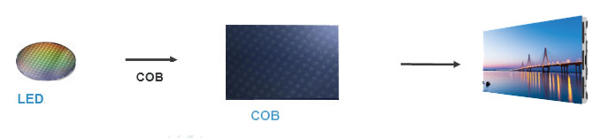
What is COB Packaging?
COB packaging is a technology that directly mounts LED chips onto a PCB. Compared to traditional SMD packaging, COB offers higher integration density, improved heat dissipation, enhanced stability, higher production efficiency, and lower costs. These advantages make COB a promising solution for advanced Mirco LED display applications.
COB Packaging Process Flow
Wafer Expansion
Place LED wafers onto an expansion ring, then position the ring on a backside adhesive coating machine;pre-coated with silver paste for expansion.
Backside Adhesive Coating
Transfer the expanded wafer ring to a backside adhesive coating machine. A dispensing machine applies a precise amount of silver paste onto the PCB.
Die Bonding
Load the silver paste-coated wafer ring into a die-bonding fixture. Under a microscope, operators use a die-bonding tool to manually place LED chips onto the PCB.
Curing
Place the PCB with bonded chips into a thermal cycling oven. Maintain a constant temperature to solidify the silver paste, then remove the PCB.
Wafer Encapsulation
Use a dispensing machine to apply red or black adhesive to designated areas on the PCB. An anti-static device precisely positions the wafer onto the adhesive.
Film Lamination
Cover the display with a pre-cut protective film ;using specialized lamination equipment to enhance performance and durability.
Final Curing
Return the encapsulated PCB to the thermal cycling oven. Adjust curing time based on specific process requirements.
Post-Assembly Testing
Conduct comprehensive quality inspections to make the COB display meets performance and reliability standards.
Advantages of COB Packaging Technology

SightLED’s COB LED displays support multiple display modes and color calibration features. They can be tailored to diverse application.
High Brightness
Brighter and sharper images; enhancing overall display clarity.
High Contrast Ratio
Improves contrast performance; achieving deeper blacks, purer whites, and more vibrant colors for exceptional visual impact.
Extended Lifespan
With superior heat dissipation and stability, COB LED displays exhibit longer operational lifespans, reducing maintenance costs and replacement frequency.
Enhanced Thermal Management
COB packaging integrates LED chips directly onto the PCB, where heat is rapidly dissipated through the board’s copper foil. Strict process controls ensure optimal copper foil thickness, combined with an immersion gold finish, minimizing light decay. This design drastically reduces dead pixels and extends product longevity.
Durability & Easy Maintenance
Smooth, Hardened Surface: The flat and robust LED dot matrix resists scratches and impacts.
Repairable Pixel-Level Defects: Individual faulty pixels can be repaired without replacing entire modules.
Effortless Cleaning: No protective lens required; dust or stains can be wiped away with water or a cloth.
All-Weather Reliability
Good waterproofing, moisture resistance, corrosion protection, dustproofing, anti-static performance, oxidation resistance, and UV stability. They operate flawlessly in extreme temperatures ranging from -20°C to +60°C, ensuring reliability in harsh environments.
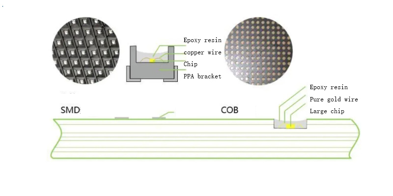
COB Vs.SMD Packaging
SMD Packaging
SMD refers to surface-mount components used in Surface Mount Technology . In the early stages of printed circuit board manufacturing, through-hole assembly was entirely manual. While early automated machines could place simple pin components, complex parts still required manual placement for wave soldering.
The introduction of surface-mount components around two decades ago marked a new era. From passive components to active devices and integrated circuits, nearly all components eventually adopted SMD packaging for compatibility with pick-and-place assembly systems. For years, it was assumed that all pin-based components would ultimately transition to SMD packaging.
Key Features of SMD Packaging:
(1) High Assembly Density: SMD components reduce product size and weight by 40–60% and 60–80%, respectively, with volumes and weights roughly 1/10th of traditional through-hole components.
(2) Enhanced Reliability: Superior vibration resistance and lower solder joint defect rates.
(3) Improved High-Frequency Performance: Reduced electromagnetic and radio-frequency interference.
(4) Cost Efficiency: Automation-friendly processes cut costs by 30–50%, saving materials, energy, labor, and time.
Technological Differences
COB Packaging involves directly bonding LED chips to PCB solder pads using conductive and insulating adhesives. After electrical performance testing, the chips are encapsulated with epoxy resin.
SMD Packaging secures LED chips to lamp bead carrier solder pads with adhesives, followed by similar electrical testing and epoxy encapsulation. Additional steps include spectral binning, dicing, and tape-and-reel packaging before shipment to display manufacturers.
Production Efficiency Comparison
COB packaging shares similar processes with traditional SMD in die bonding and wire bonding. However, COB outperforms SMD in dispensing, separation, binning, and packaging. Labor and manufacturing costs account for ~15% of material costs in SMD, compared to ~10% for COB, yielding a 5% cost reduction.
Advantages and Limitations
While SMD packaging reliably produces high-quality LED beads, its multi-step process incurs higher costs, including transportation, storage, and quality control between packaging and display manufacturers. Critics of COB argue its technical complexity leads to lower first-pass yields and irreparable defects.
However, current COB technology achieves first-pass yields of ~70% for 0.5K integration, ~50% for 1K, and ~30% for 2K. Even modules failing initial tests typically exhibit only 1–5 defective points, with fewer than 5% exceeding this threshold. Pre-encapsulation testing and rework enable final yields of 90–95%. Advances in equipment and process control continue to improve these metrics, supported by post-encapsulation defect repair capabilities.
Comparison of Low Thermal Resistance and Light Quality Performance
Low Thermal Resistance:
Traditional SMD packaging follows a system thermal resistance path: chip → die-bonding adhesive → solder joint → solder paste → copper foil → insulation layer → aluminum substrate.
COB packaging simplifies this to: chip → die-bonding adhesive → aluminum substrate.
The thermal resistance of COB packaging is significantly lower than that of traditional SMD packaging, greatly extending LED lifespan.
Light Quality:
Traditional SMD packaging mounts multiple discrete devices onto a PCB to form a light source assembly, which often results in issues such as point light sources, glare, and ghosting.
COB packaging provides a uniform surface light source; a wide adjustable viewing angle, minimizing light refraction loss.
Technical Analysis and Evaluation
| Project | COB Packaging | Traditional SMD Packaging |
|---|---|---|
| Production Efficiency | Solid crystal, wire bonding efficiency is equivalent to traditional SMD; post-process dot glue, separation, light splitting, packaging efficiency is higher than traditional SMD | Production efficiency is lower than COB packaging |
| Thermal Resistance | Chip – solid crystal glue – aluminum material (low thermal resistance) | Chip – solid crystal glue – solder joint – solder paste – copper foil – insulation layer – aluminum material (thermal resistance is higher than COB packaging) |
| Optical Quality | Large viewing angle and easy to adjust, reducing light output refraction loss | Discrete device combinations have issues of dot light and glare |
| Application | No need for patch and reflow soldering processes; COB light source can be directly applied to lamps | LED devices need to be first patched and then fixed on PCB boards through reflow soldering |
| Cost | Lower cost | Increased costs for bracket, solder paste, patching, and reflow soldering processes |
Technical Implementation Difficulty:
SMD Packaging: A mature technology with years of practical experience; established processes, and scale. Implementation is relatively straightforward.
COB Packaging: A novel multi-chip integrated technology requiring innovation in production equipment, process tools, testing methods, and technical expertise. High technical barriers exist, with the current major challenge being improving first-pass yield. While technically demanding, COB is achievable but requires significant effort.
Failure Rate Control at Delivery:
Both COB and SMD packaging can achieve near-zero failure rates when delivered to customers.
Cost Control:
Theoretically, COB holds a slight cost advantage. However, due to limited production scale, SMD currently remains more cost-effective.
Reliability Risks:
SMD Packaging: Quadruple or hexagonal brackets introduce technical challenges and reliability risks, such as soldering yield for massive bracket pins during reflow and outdoor protection for pins.
COB Packaging: Eliminates brackets, reducing technical difficulties and risks. Key challenges include ensuring no failure points during reflow soldering of IC driver chips and achieving consistent module ink coloration.
User-Friendliness in Applications:
COB Packaging:
- LEDs are epoxy-sealed on PCBs;
- Exceptional physical properties:
- Compressive strength: 8.4 kg/mm²
- Shear strength: 4.2 kg/mm²
- Impact strength: 6.8 kg·cm/cm²
- Hardness: Shore D 84
Resistant to static electricity, collisions, impacts, bending, abrasion, and easy to clean. Highly durable and human-friendly.
SMD Packaging: LEDs are soldered via bracket pins to PCBs, with weaker physical strength. Vulnerable to touch-induced static failure and mechanical damage, offering lower user-friendliness.
Critical Note on SMD Challenges:
To cut costs, some SMD manufacturers reduce carrier frame heights, inadvertently increasing encapsulation process complexity and lowering yield rates. This compromises reliability and raises encapsulation costs, ultimately negating intended savings.
Conclusion
We have introduced the COB manufacturing process. Compared with previous years, COB manufacturing process has made great breakthroughs, and it can be said that the technology is very mature. And the COB dislay price is very affordable. If you need ultra-HD video wall display, why not consider this new technology? If you need COB LED display, feel free to contact us.